Low Dropout Regulator (LDO) Design
Course: ECE 483 - Analog IC Design
Authors: Sayankar, Rutvik and Patel, Dev
This project involved designing and simulating an LDO to meet specific input/output/load criteria while ensuring precise DC load and line regulation.
Design Highlights
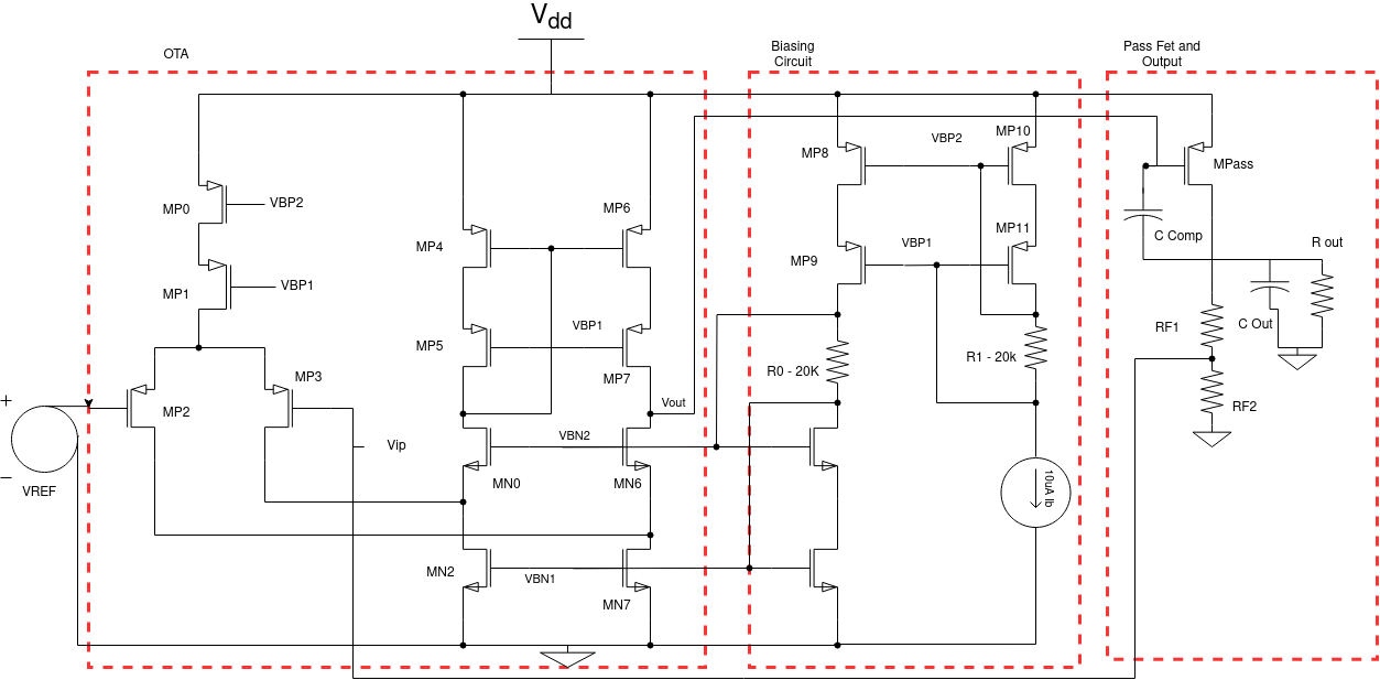
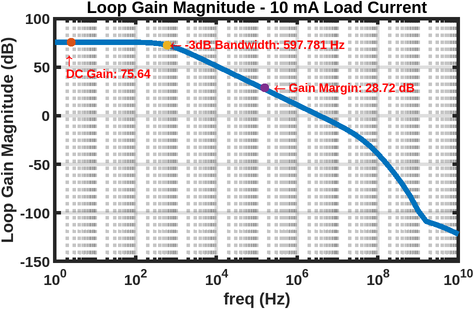
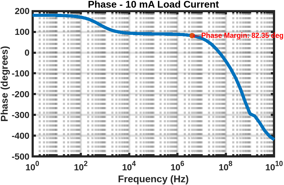
- Topology: Telescopic Cascode OTA for superior output swing and stability.
- Compensation Capacitor: Optimized for phase margin and loop gain.
- Performance: Achieved 15.55 µV/mA load regulation and a worst-case PSR of -1.42 dB.
Simulation Results
Key parameters such as load regulation, line regulation, and power supply rejection were analyzed to ensure optimal performance. The design met stringent specifications for high-efficiency voltage regulation.